
General
There is a little-known method of generating a bias voltage which is called "back-biasing". It is an inexpensive and easy method of generating a negative bias supply for an amplifier which uses a full-wave, center-tapped rectifier, either tube or solid-state. It is particularly useful when it is also desirable to lower the plate voltage supply by fifteen to twenty volts or more.
How does it work?
Back biasing is one of the simplest methods of generating a negative supply voltage. All that is needed is a resistor in series with the center-tap of the B+ supply, bypassed with a large enough capacitance to "smooth out" the full-wave voltage ripples that result from the conduction on each half of the sine wave. This circuit was particularly useful in the old days when small silicon rectifiers weren't available, because a vacuum tube rectifier could be used for the B+ supply and the negative bias supply could be generated without any additional diodes.
The circuit below illustrates this biasing method:

The plot shown below illustrates the current flow in the center-tap of the transformer. The red trace is the current, the green trace is the input voltage, scaled down to show the relationship between the current flow and the input AC voltage cycle. Note that the current flows in one direction only, into the center tap. This unidirectional, full-wave rectified current flow produces a voltage drop across the back-bias resistor, which is inserted between ground and the center-tap of the transformer. Since the current flows from ground through the resistor, this creates a voltage drop from ground to the other end of the resistor, which is connected to the center-tap of the transformer. This voltage drop produces a negative voltage at the center-tap.

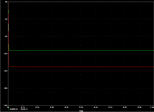
This trace shows the voltage developed at the center-tap of the transformer, due to the current dropped across the resistor. Note the voltage is only negative-going, full-wave rectified pulses. This rectified voltage can be filtered and used as the negative bias supply.

The filter capacitor removes the ripples from the supply, and produces a relatively clean DC bias voltage as shown in the plot below. The red trace illustrates the partial filtering obtained by C1 in the above schematic, and the green trace illustrates the final bias supply voltage after the second stage of filtering provided by R2 and C3. If the residual ripple is too large, C1, R2 and/or C3 can be increased to provide greater filtering. However, if the capacitors are made too large, the supply with take a long time to come up to the correct voltage, which could be detrimental to the life of the tubes. Note the ramp-up time shown in the plot below, using the values shown in the above schematic:

The design process
In order to calculate the required component values, it is necessary to know the value of the current drawn from the B+ supply at idle. Once this is known, the value of R1, the back-bias resistor, can be easily determined using Ohm's law. For example, assuming the supply is designed for use with a fixed-bias push-pull EL84 output stage, with a nominal current draw at idle of around 68mA. It is desired to have a bias supply range from -9V to -13V, nominally -11V.First, R1 is determined by dividing the desired voltage by the idle current. In the above case, we want 15V at 68mA, which gives a resistance of 15V/68mA = 220 ohms. 15V was chosen to limit the dissipation in the back-bias resistor while providing some overhead to allow for the voltage drop that occurs in further filtering of the supply by R2/C3. Note that the bias supply really doesn't have to provide any current to speak of, because the grids of the output tubes normally don't draw any current. The power rating of R1 is calculated again using Ohm's law, by dividing the voltage squared by the resistance. In this case, it is equal to 152/220 = 1W. In order to allow for possible increases in dissipation at full power, and to allow some safety margin, a 3W or 5W resistor should be used.
A suitable potentiometer is chosen next. A value of 10K is good, because it is much larger than the back-bias resistor, and won't draw much current or dissipate much power. R2 and R3 are then calculated to give the desired bias adjustment range, with the nominal value of 11V when the pot is set to center, or 5K. Note that the potentiometer is configured such that if the wiper contact should fail, the bias supply will go to the full negative value, which will protect the output tubes in the event of such a failure. Also be sure to note the correct orientation of the filter capacitors, including the one across the back-bias resistor and the post-filter capacitor, both of which have the positive terminal connected to ground, instead of the usual arrangement where the negative terminal is grounded.
What's the catch?
The problem with the above circuit is that the voltage drop across the back-bias resistor, R1, is dependent upon the amount of current drawn by the B+ supply. This poor regulation limits the circuit's usefulness, unless "sag" is desired in both the plate supply and the bias supply. The regulation can be quite good for a true class A amplifier, because the variation in current between idle and full output power is minimal. In a class AB or class B circuit, however, the current variation between idle and full power can be quite large, which will cause the bias supply to be modulated with the signal voltage.
A better method - the zener back-bias circuit
There is a better method of utilizing back-bias which has none of the drawbacks of the above circuit. This method uses a series zener diode to replace the back-bias resistor. The dynamic impedance of a zener diode is very low, on the order of 5-20 ohms or so, depending, of course, on the particular part and the current flowing through it. The rapid reverse breakdown characteristic, which gives this low impedance, is what makes zeners so useful in voltage regulation applications, where they are generally used as shunt regulators. They are also used as series voltage dropping elements, because the reverse drop is relatively constant over a wide range of current flow. The series regulator configuration is used in this circuit, as shown in the schematic below. This circuit has the distinct advantage of providing a regulated bias supply with only one zener diode and fewer components than the "usual" bias supply circuits. It also provides a steady 15V drop in the main B+ supply, which is independent of current draw. This is very useful in cases where the supply voltage is a bit too high for the tubes being used. The zener power rating must be chosen for the max dissipation of the circuit, by multiplying the zener voltage by the max average current of the amplifier. In the circuit shown below, the idle dissipation is equal to 68mA * 15V = 1W. In order to accommodate the increase in current draw at full power, and afford a safety margin, a 5W zener should be used. It is useful to note that the dissipation goes up as the zener voltage is increased, which limits this circuit to lower-power amplifiers that require small bias voltages, such as those using EL84 tubes, unless a power zener is used, which then must be well heat-sinked to the chassis. A good alternative to large power zeners is to use multiple lower-voltage zeners in series to achieve the required voltage drop.

Following is a plot showing the difference between the zener back-bias circuit and the resistor back-bias circuit. The green trace is the zener output bias voltage, and the red trace is the raw zener supply at the center tap. The purple trace is the resistor back-bias output voltage, and the yellow trace is the raw back-bias resistor supply. Note the much faster startup of the zener supply, and the lower residual ripple voltage, as well as the tight regulation as the circuit starts up, compared to the large overshoot of the resistive method.

This circuit can be safely used even in amplifiers that have a standby switch which shuts off the current to the output tubes, because the bias voltage comes up quickly, within 100mS, provided the post-filter time constant shown above is used. Large filter capacitors are not necessary and should be avoided, because they will slow down the ramp-up time of the bias supply. If the standby switch is positioned after the first main filter capacitor, and a "bleeder" resistor is used, the bias voltage will stay on during standby.
An even better method - the improved zener back-bias circuit
While the above circuit is a great improvement on the resistor biasing method, it can be carried one step further by changing the connection of the main filter capacitor. In the above circuit, all the high-current charging pulses that "fill up" the capacitor must pass through the zener diode, which means that a capacitor must be placed across the zener diode to filter them out (C1 - the 680uF cap in the above schematic). If you instead connect the main filter cap ground to the center-tap of the transformer instead of the chassis ground, all these high-current charging pulses are contained in a loop around the transformer, through the rectifier, down through the filter cap, and back to the transformer CT, and they don't pass through the zener diode at all. The only current that passes through the zener diode is the current drawn by the amplifier, which is much steadier on average than the capacitor charging current. This allows you to completely do away with the zener filter cap, and results in a very fast regulated bias supply that needs no filter caps whatsoever! In some cases, however, a small capacitor may be necessary across the zener diode to prevent noise, particularly when switching the amp in and out of standby.Note that you must keep a small load current on the output at all times, or the zener bias voltage won't stay regulated. If the standby switch cuts off the voltage to the amp, there will be no current flow through the zener and the bias voltage will drop to zero. The speed of the bias circuit (since is doesn't use filter capacitors) is sufficient to not cause a problem, but if you would like to keep the bias voltage at the correct value with the amp in standby, a "bleeder" resistor should be connected from the filter caps to ground (not across the filter caps as they are usually connected). The schematic shown below incorporates this bleeder resistor (R4).
One last note: if you are using a "star ground" system with this bias circuit, the first star point will be the point at which the zener diode is grounded.

Following is a plot showing the improved zener back-bias circuit. The green trace is the zener output bias voltage, and the red trace is the raw zener supply at the center tap. Note the even faster startup of the zener supply, and the almost non-existent residual ripple voltage (compared to the red trace in the previous image), as well as the even tighter regulation as the circuit starts up.
And now the catch - too good to be true?
The above circuit produces what at first glance seems to be the ideal bias voltage generator. Completely regulated, no filter capacitors needed - so what's the catch? Well, the catch is that regulating the bias voltage without regulating the plate and/or screen supplies has an inherent problem. If the AC mains voltage rises or falls from the nominal voltage, the bias voltage will not track the changes in the plate/screen voltage. This means that as the plate voltage rises (and more importantly, as the screen voltage rises, which has more control over the plate current than the plate voltage in a pentode), the bias voltage remains at the same regulated voltage, which means that the bias current will increase. If the supply voltage decreases, the bias voltage will still remain constant, but the bias current will decrease due to the lower screen and plate voltages. Since the bias current increases with an increase in plate voltage, the plate dissipation will increase with an increase in the AC mains supply voltage, and likewise, the plate dissipation will decrease with a decrease in the AC mains supply voltage. Basically, the bias current is dependent on the AC mains supply voltage, which is not a good thing if there are large variations in the mains supply voltage. In practice, it is not too bad, though, because the wall voltage doesn't usually vary a great deal, and when it does, it usually is on the low side, rather than the high side, which means the bias current will be lower, and plate dissipation will not be too high.The best solution to the above problem is to regulate the screen voltage, using a high-voltage zener or active regulator circuit. If the screen voltage is held constant, and the bias voltage is held constant, the plate voltage can be varied over a wide range without affecting the bias current at all. The varying plate voltage will still allow the amplifier's "sag" to be a function of plate voltage, while maintaining rock-steady bias current. However, screen regulation adds complexity and cost to the amplifier, so this is usually not done, except in cases where the absolutetly quiet operation and zero hum of a screen regulated supply is needed.
Another solution - a bit of the old with a bit of the new:
Another very simple solution to the above regulation problem brings us back full circle to the original design, with one new twist - the location of the ground on the main filter supply cap. The schematic shown below illustrates this method:

The tightly regulated zener diode is replaced by a resistor which is selected to give the desired voltage drop for the bias circuit. Now, if the AC mains voltage increases, and the plate/screen voltages increase, the amplifier will draw more current from the supply. This increased current draw will increase the voltage drop across R1, the bias resistor, which will in turn increase the negative bias voltage and decrease the plate current back to near the original value. Likewise, if the AC mains voltage decreases, the decreased plate current draw will decrease the negative bias voltage, which increases the plate current in opposition to the change, keeping it relatively constant. It turns out that the above circuit will hold the bias current, which is nominally set to 28mA, to a range of around +/-1.3mA with an AC mains variation from 115V to 125V, nominally 120V.
Adjustable cathode bias without the cathode resistor?
A drawback of this new resistive back-bias design, which is not exhibited by the zener back-bias method, is that variations in current drawn by the output stage during normal operation will cause variations in the bias voltage. This is not necessarily a bad thing. If you think about what this circuit is doing for a minute, you will realize that what we have here is effectively cathode biasing which is adjustable with a standard trimpot as you would normally adjust fixed bias! We have simply taken the current-dependent, voltage-varying element (the cathode resistor) and moved it from the cathode to the plate circuit, and moved the controlling voltage from the cathode to the grid, which results in the same behavior, since the tube current depends on the relative grid-to-cathode potential. This modulation of the bias voltage by the plate current requires the addition of a filter capacitor across the back-bias resistor, similar to the filter capacitor across the cathode resistor in a cathode-biased design (the zener back-bias circuit didn't need it because of the extremely low zener impedance). A simple modification to the above circuit will allow "effective" cathode biasing with the added enhancements of adjustable bias and balance controls, which is very difficult to implement in a standard cathode-biasing system, because it would require adjustable power resistors or large, high-wattage wirewound pots.
Disclaimer:
The above circuits may be freely used in either private or commercial amplifiers, or copied and distributed, provided credit is given to the author.
Copyright © 2000, 2001 Randall Aiken. May not be reproduced in any form without written approval from Aiken Amplification.
Revised 02/18/14